Comprehensive Optical Wafer Testing For μleds At A Single Test Station
Find inspiration for Comprehensive Optical Wafer Testing For μleds At A Single Test Station with our image finder website, Comprehensive Optical Wafer Testing For μleds At A Single Test Station is one of the most popular images and photo galleries in Comprehensive Optical Wafer Testing For μleds At A Single Test Station Gallery, Comprehensive Optical Wafer Testing For μleds At A Single Test Station Picture are available in collection of high-quality images and discover endless ideas for your living spaces, You will be able to watch high quality photo galleries Comprehensive Optical Wafer Testing For μleds At A Single Test Station.
aiartphotoz.com is free images/photos finder and fully automatic search engine, No Images files are hosted on our server, All links and images displayed on our site are automatically indexed by our crawlers, We only help to make it easier for visitors to find a free wallpaper, background Photos, Design Collection, Home Decor and Interior Design photos in some search engines. aiartphotoz.com is not responsible for third party website content. If this picture is your intelectual property (copyright infringement) or child pornography / immature images, please send email to aiophotoz[at]gmail.com for abuse. We will follow up your report/abuse within 24 hours.
Related Images of Comprehensive Optical Wafer Testing For μleds At A Single Test Station
Comprehensive Optical Wafer Testing For μleds At A Single Test Station
Comprehensive Optical Wafer Testing For μleds At A Single Test Station
1200×630

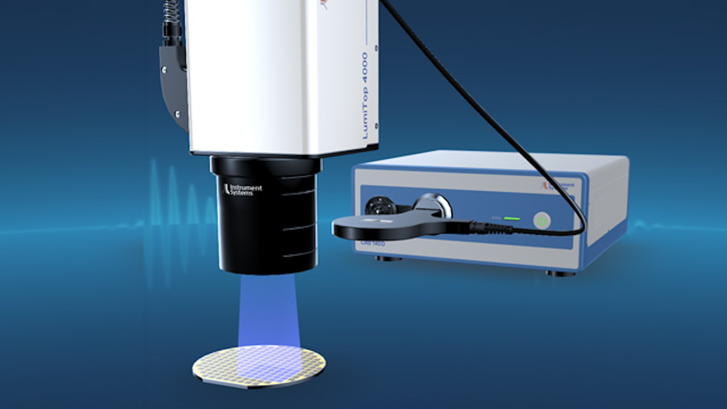
Lumitop 4000 Comprehensive Optical Wafer Testing For μleds — Led
Lumitop 4000 Comprehensive Optical Wafer Testing For μleds — Led
960×640

Comprehensive Optical Wafer Testing For μleds At A Single Test Station
Comprehensive Optical Wafer Testing For μleds At A Single Test Station
1000×890
Vcsel And Microled Measurements Optical Wafer Probe Stations
Vcsel And Microled Measurements Optical Wafer Probe Stations
720×482
Optoelectronic Wafer Probe Equipment Photonic Wafer Level Probe Test
Optoelectronic Wafer Probe Equipment Photonic Wafer Level Probe Test
1000×880


Color Online A Picture And B Cross Sectional Schematic Of The
Color Online A Picture And B Cross Sectional Schematic Of The
850×345

Performing Comprehensive Wafer Inspection With Non Contact 3d Optical
Performing Comprehensive Wafer Inspection With Non Contact 3d Optical
774×575
Instrument Systems Comprehensive Optical Wafer Testing For Leds At A
Instrument Systems Comprehensive Optical Wafer Testing For Leds At A
768×401

Success Story Semiautomatic Optoelectronics Wafer Test System Light
Success Story Semiautomatic Optoelectronics Wafer Test System Light
2646×1771

Guide To Wafer Probe Testing Systems
Guide To Wafer Probe Testing Systems
1500×1333

Optoelectronic Wafer Probe Equipment Photonic Wafer Level Probe Test
Optoelectronic Wafer Probe Equipment Photonic Wafer Level Probe Test
500×440
Optical System For Inspection Of Micro Structured Wafer Lighttrans
Optical System For Inspection Of Micro Structured Wafer Lighttrans
1406×727

Optoelectronic Wafer Prober Vcsels Success Story
Optoelectronic Wafer Prober Vcsels Success Story
2650×1986

Guide To Wafer Probe Testing Systems
Guide To Wafer Probe Testing Systems
1224×893

Performing Comprehensive Wafer Inspection With Non Contact 3d Optical
Performing Comprehensive Wafer Inspection With Non Contact 3d Optical
1200×808
A Comprehensive Guide To Test Wafers What Are They And Why Are They
A Comprehensive Guide To Test Wafers What Are They And Why Are They
770×513

Probe Positioners For Dc Rf And Optical Wafer Test Formfactor Inc
Probe Positioners For Dc Rf And Optical Wafer Test Formfactor Inc
720×480

Ficontec Electro Optical Wafer Level Test Systems For Pics Youtube
Ficontec Electro Optical Wafer Level Test Systems For Pics Youtube
1280×720

Guide To Wafer Probe Testing Systems
Guide To Wafer Probe Testing Systems
1500×1275
Fiberless Optical Stimulation Using μleds A Gan μleds Grown On
Fiberless Optical Stimulation Using μleds A Gan μleds Grown On
850×353

Testing The Waters A Comprehensive Guide To Test Wafer Solutions
Testing The Waters A Comprehensive Guide To Test Wafer Solutions
768×512

Guide To Wafer Probe Testing Systems
Guide To Wafer Probe Testing Systems
1800×1199

Developing Silicon Photonics Technologies With A Wafer Level Test Station
Developing Silicon Photonics Technologies With A Wafer Level Test Station
1929×1085
Everything Asic Designing Wafer Testing Adsantec
Everything Asic Designing Wafer Testing Adsantec
772×600


Kla Tencor Introduces Comprehensive Wafer Inspection And Review
Kla Tencor Introduces Comprehensive Wafer Inspection And Review
2086×2700

Guide To Wafer Probe Testing Systems
Guide To Wafer Probe Testing Systems
2412×1352
Guide To Wafer Probe Testing Systems
Guide To Wafer Probe Testing Systems
1800×2496

Increasing Wafer Probe Testing Throughput By Means Of Servo Elmo
Increasing Wafer Probe Testing Throughput By Means Of Servo Elmo
4639×3197

Kla Tencor Introduces Comprehensive Wafer Inspection And Review
Kla Tencor Introduces Comprehensive Wafer Inspection And Review
2700×2032

Fiberless Optical Stimulation Using μleds A Gan μleds Grown On
Fiberless Optical Stimulation Using μleds A Gan μleds Grown On
640×640

Advanced Optoelectronics Wafer Prober And Test Applications
Advanced Optoelectronics Wafer Prober And Test Applications
1318×882

Fully Automated Very Compact Led Wafer Inspection Metrology System
Fully Automated Very Compact Led Wafer Inspection Metrology System
1280×720
