Exploring The Different Types Of Pcb Layers And Its Purpose
Find inspiration for Exploring The Different Types Of Pcb Layers And Its Purpose with our image finder website, Exploring The Different Types Of Pcb Layers And Its Purpose is one of the most popular images and photo galleries in Insulation Layers Of Pcb Lamenate Gallery, Exploring The Different Types Of Pcb Layers And Its Purpose Picture are available in collection of high-quality images and discover endless ideas for your living spaces, You will be able to watch high quality photo galleries Exploring The Different Types Of Pcb Layers And Its Purpose.
aiartphotoz.com is free images/photos finder and fully automatic search engine, No Images files are hosted on our server, All links and images displayed on our site are automatically indexed by our crawlers, We only help to make it easier for visitors to find a free wallpaper, background Photos, Design Collection, Home Decor and Interior Design photos in some search engines. aiartphotoz.com is not responsible for third party website content. If this picture is your intelectual property (copyright infringement) or child pornography / immature images, please send email to aiophotoz[at]gmail.com for abuse. We will follow up your report/abuse within 24 hours.
Related Images of Exploring The Different Types Of Pcb Layers And Its Purpose

What Is Lamination Process In Pcb Fabrication Pcb Hero
What Is Lamination Process In Pcb Fabrication Pcb Hero
1000×667
Pcb Circuit Board Structure Of The Even Numbered Layers Of Pcbs
Pcb Circuit Board Structure Of The Even Numbered Layers Of Pcbs
768×475

Pcb Laminate Materials Types Of Laminate Materials In Pcb
Pcb Laminate Materials Types Of Laminate Materials In Pcb
1000×711


Pcb Insulation And Its Importance Between Layers
Pcb Insulation And Its Importance Between Layers
1024×544

Pcb Stack Up Guide And Examples San Francisco Circuits
Pcb Stack Up Guide And Examples San Francisco Circuits
1600×639

Pcb Insulation Non Conductive Layers For Separating Pcb Electrical
Pcb Insulation Non Conductive Layers For Separating Pcb Electrical
1000×554

Pcb Insulation And Its Importance Between Layers
Pcb Insulation And Its Importance Between Layers
1096×640

Pcb Layers And Printed Circuit Board Working Layers
Pcb Layers And Printed Circuit Board Working Layers
769×262
Pcb Layers Explained Everything You Need To Know
Pcb Layers Explained Everything You Need To Know
1225×641
Pcb Laminate The Ultimate Guide For Beginners Ibe Electronics
Pcb Laminate The Ultimate Guide For Beginners Ibe Electronics
1280×720

An Introduction To The Pcb Lamination Process By Pcbgogo
An Introduction To The Pcb Lamination Process By Pcbgogo
530×310

Insulation In Pcb Manufacturing Advanced Technology And Manufacturing
Insulation In Pcb Manufacturing Advanced Technology And Manufacturing
1826×913

An Ultimate Guide To Pcb Laminate Materials For Fabrication Hillman
An Ultimate Guide To Pcb Laminate Materials For Fabrication Hillman
1024×543

The Importance Of Pcb Laminate Technology For Pcb Layout Grandes Blog
The Importance Of Pcb Laminate Technology For Pcb Layout Grandes Blog
437×621

What Is The Pcb Lamination Process In Manufacturing Techsparks
What Is The Pcb Lamination Process In Manufacturing Techsparks
800×533

Pcb Substrates Knowing Pcb Dielectric Materials Sierra Circuits
Pcb Substrates Knowing Pcb Dielectric Materials Sierra Circuits
799×452


Pcb Structure A Detailed Introduction To Its Layers Ibe Electronics
Pcb Structure A Detailed Introduction To Its Layers Ibe Electronics
1000×500
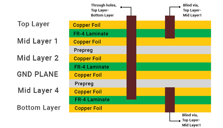
Exploring The Different Types Of Pcb Layers And Its Purpose
Exploring The Different Types Of Pcb Layers And Its Purpose
750×430

Sequential Lamination The Backbone Of Pcb Fabrication
Sequential Lamination The Backbone Of Pcb Fabrication
675×453

Aluminum Pcb Pcb Prototype The Easy Way Pcbway
Aluminum Pcb Pcb Prototype The Easy Way Pcbway
785×449

Exploring The Different Types Of Pcb Layers And Its Purpose
Exploring The Different Types Of Pcb Layers And Its Purpose
750×500

Pcb Design Characteristics Details And Types Of Pcb Substrates
Pcb Design Characteristics Details And Types Of Pcb Substrates
920×323

Pcb Laminate The Ultimate Guide For Beginners Ibe Electronics
Pcb Laminate The Ultimate Guide For Beginners Ibe Electronics
1000×522
Pcb Laminate The Ultimate Guide For Beginners Ibe Electronics
Pcb Laminate The Ultimate Guide For Beginners Ibe Electronics
1000×522

Pcb Insulation An Essential Aspect Of Pcb Production
Pcb Insulation An Essential Aspect Of Pcb Production
1000×449

Pcb Substrates Knowing Your Pcb Dielectric Materials Sierra Circuits
Pcb Substrates Knowing Your Pcb Dielectric Materials Sierra Circuits
610×312

Pcb Layers Fundamentals And Simple Introducing Wellpcb
Pcb Layers Fundamentals And Simple Introducing Wellpcb
602×443

Common Pcb Laminate Structure For Pcb Emc Design
Common Pcb Laminate Structure For Pcb Emc Design
586×274

Insulation Metal Substrate Aluminum Based Copper Clad Laminate Sheet
Insulation Metal Substrate Aluminum Based Copper Clad Laminate Sheet
693×392
