Figure 1 Standard Wafer Test 3d Incites
Find inspiration for Figure 1 Standard Wafer Test 3d Incites with our image finder website, Figure 1 Standard Wafer Test 3d Incites is one of the most popular images and photo galleries in Figure 1 Standard Wafer Test 3d Incites Gallery, Figure 1 Standard Wafer Test 3d Incites Picture are available in collection of high-quality images and discover endless ideas for your living spaces, You will be able to watch high quality photo galleries Figure 1 Standard Wafer Test 3d Incites.
aiartphotoz.com is free images/photos finder and fully automatic search engine, No Images files are hosted on our server, All links and images displayed on our site are automatically indexed by our crawlers, We only help to make it easier for visitors to find a free wallpaper, background Photos, Design Collection, Home Decor and Interior Design photos in some search engines. aiartphotoz.com is not responsible for third party website content. If this picture is your intelectual property (copyright infringement) or child pornography / immature images, please send email to aiophotoz[at]gmail.com for abuse. We will follow up your report/abuse within 24 hours.
Related Images of Figure 1 Standard Wafer Test 3d Incites


Figure 1 From Advanced Wafer Thinning Technology And Feasibility Test
Figure 1 From Advanced Wafer Thinning Technology And Feasibility Test
1292×760

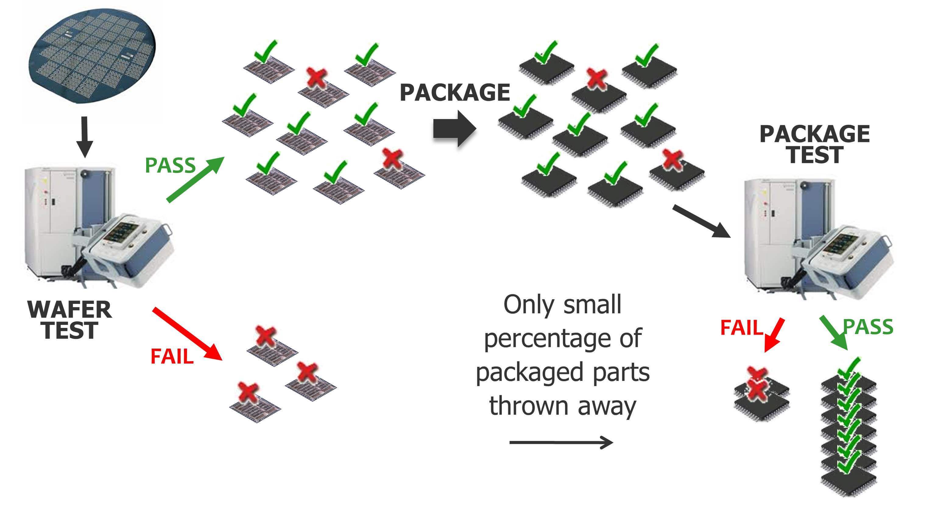
How Is Testing Completed In Silicon Wafer Manufacturing Process
How Is Testing Completed In Silicon Wafer Manufacturing Process
2000×1333


Figure 1 From Test Method For Wafer Bond Strength Measurements Using
Figure 1 From Test Method For Wafer Bond Strength Measurements Using
1256×714

A Look At Imecs Two Step Wafer Level Mold Process 3d Incites
A Look At Imecs Two Step Wafer Level Mold Process 3d Incites
433×575

Figure 1 From 3d Large Scale Integration Technology Using Wafer On
Figure 1 From 3d Large Scale Integration Technology Using Wafer On
812×578

Figure 1 From 3d Integration Technology Using Hybrid Wafer Bonding And
Figure 1 From 3d Integration Technology Using Hybrid Wafer Bonding And
604×420

Understanding Wafer Applications In Surface Metrology 3d Incites
Understanding Wafer Applications In Surface Metrology 3d Incites
1200×474

Figure 1 From 300 Mm Wafer 3d Integration Technology Using Hybrid Wafer
Figure 1 From 300 Mm Wafer 3d Integration Technology Using Hybrid Wafer
644×992
Ev Group Unveils Hybrid Die To Wafer Bonding Activation Solution To
Ev Group Unveils Hybrid Die To Wafer Bonding Activation Solution To
2560×1719

Discover Wafer Universe Your Premier Source For Standardized Wafers
Discover Wafer Universe Your Premier Source For Standardized Wafers
540×315

Market Outlook For Permanent Wafer Bonding 3d Incites
Market Outlook For Permanent Wafer Bonding 3d Incites
1990×1493
Indium Corporation Wafer Flux Ws 3543 3d Incites
Indium Corporation Wafer Flux Ws 3543 3d Incites
667×1000
Pwg5™ The Complete Wafer Geometry System For Ic Fabs Innovation Kla
Pwg5™ The Complete Wafer Geometry System For Ic Fabs Innovation Kla
1280×381


Screenshot 2022 05 24 At 09 27 55 Ers Electronic Introduces Probesense
Screenshot 2022 05 24 At 09 27 55 Ers Electronic Introduces Probesense
768×432

How To Prevent High Wafer Warpage In Fan In And Fan Out Wafer Level
How To Prevent High Wafer Warpage In Fan In And Fan Out Wafer Level
1200×720

C V Curves Of 3d Test Diodes From Wafers Of Two Different Active
C V Curves Of 3d Test Diodes From Wafers Of Two Different Active
580×580

Figure 1 From Wafer Level Process Variation Driven Probe Test Flow
Figure 1 From Wafer Level Process Variation Driven Probe Test Flow
658×396
Jlpea Free Full Text Three Dimensional Wafer Stacking Using Cu Tsv
Jlpea Free Full Text Three Dimensional Wafer Stacking Using Cu Tsv
2722×2254
Probing Questions At The Ieee 3d Ic Test Workshop 3d Incites
Probing Questions At The Ieee 3d Ic Test Workshop 3d Incites
1512×1134


Pdf 3d Printed Optics For Wafer Scale Probing Semantic Scholar
Pdf 3d Printed Optics For Wafer Scale Probing Semantic Scholar
602×370
Semiconductor Back End Process 1 Semiconductor Testing
Semiconductor Back End Process 1 Semiconductor Testing
1000×625
Thin Wafers High Tech In The Microelectronics 3d Incites
Thin Wafers High Tech In The Microelectronics 3d Incites
1024×622

Figure 1 From Testing Of Copper Pillar Bumps For Wafer Sort Semantic
Figure 1 From Testing Of Copper Pillar Bumps For Wafer Sort Semantic
634×674

Ssec Innovators In Single Wafer Wet Processing Tools 3d Incites
Ssec Innovators In Single Wafer Wet Processing Tools 3d Incites
500×286
Photonics Free Full Text Wafer Eccentricity Deviation Measurement
Photonics Free Full Text Wafer Eccentricity Deviation Measurement
2294×1444

What Silicon Wafer Orientation Should I Use For Research
What Silicon Wafer Orientation Should I Use For Research
1250×561

Challenges And Solutions For Silicon Wafer Bevel Defects During 3d Nand
Challenges And Solutions For Silicon Wafer Bevel Defects During 3d Nand
850×500
