Lead Frame On Chip Package Precision Stamping Cnstamping
Find inspiration for Lead Frame On Chip Package Precision Stamping Cnstamping with our image finder website, Lead Frame On Chip Package Precision Stamping Cnstamping is one of the most popular images and photo galleries in Lead Frame On Chip Package Precision Stamping Cnstamping Gallery, Lead Frame On Chip Package Precision Stamping Cnstamping Picture are available in collection of high-quality images and discover endless ideas for your living spaces, You will be able to watch high quality photo galleries Lead Frame On Chip Package Precision Stamping Cnstamping.
aiartphotoz.com is free images/photos finder and fully automatic search engine, No Images files are hosted on our server, All links and images displayed on our site are automatically indexed by our crawlers, We only help to make it easier for visitors to find a free wallpaper, background Photos, Design Collection, Home Decor and Interior Design photos in some search engines. aiartphotoz.com is not responsible for third party website content. If this picture is your intelectual property (copyright infringement) or child pornography / immature images, please send email to aiophotoz[at]gmail.com for abuse. We will follow up your report/abuse within 24 hours.
Related Images of Lead Frame On Chip Package Precision Stamping Cnstamping

Lead Frames In Semiconductor Industry Stamped Lead Frames Cnstamping
Lead Frames In Semiconductor Industry Stamped Lead Frames Cnstamping
600×400

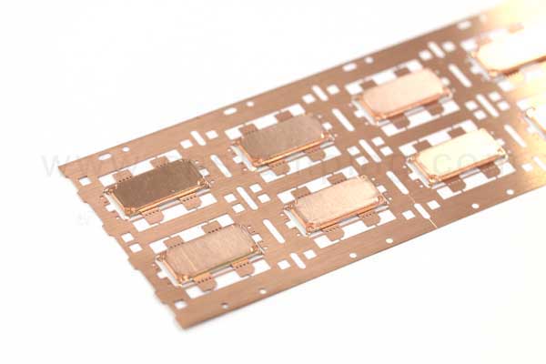
Lead Frame On Chip Package Precision Stamping Cnstamping
Lead Frame On Chip Package Precision Stamping Cnstamping
600×400

Lead Frames In Semiconductor Industry Stamped Lead Frames Cnstamping
Lead Frames In Semiconductor Industry Stamped Lead Frames Cnstamping
600×400


An 772 A Design And Manufacturing Guide For The Lead Frame Chip Scale
An 772 A Design And Manufacturing Guide For The Lead Frame Chip Scale
602×187

Parts Ic Led Stamped Lead Frame Sip 14l High Precision Stamping
Parts Ic Led Stamped Lead Frame Sip 14l High Precision Stamping
680×510

An 772 A Design And Manufacturing Guide For The Lead Frame Chip Scale
An 772 A Design And Manufacturing Guide For The Lead Frame Chip Scale
900×602

Close Epoxy Stamping On Lead Frame Stock Photo 724169938 Shutterstock
Close Epoxy Stamping On Lead Frame Stock Photo 724169938 Shutterstock
1500×1101
Parts Ic Led Stamped Lead Frame Sip 14l High Precision Stamping
Parts Ic Led Stamped Lead Frame Sip 14l High Precision Stamping
700×525

Precision Stamping Die For Lead Frame Jx09287 China Stamping Die
Precision Stamping Die For Lead Frame Jx09287 China Stamping Die
760×760
Leaded Package Qfptsop Leadframe Services Shinko Electric
Leaded Package Qfptsop Leadframe Services Shinko Electric
900×312

An 772 A Design And Manufacturing Guide For The Lead Frame Chip Scale
An 772 A Design And Manufacturing Guide For The Lead Frame Chip Scale
848×450

High Precision Lead Frames Stamped Lead Frames Wiegel Tool Works
High Precision Lead Frames Stamped Lead Frames Wiegel Tool Works
1000×1000

The Ultimate Guide To Lead Frame Anysilicon
The Ultimate Guide To Lead Frame Anysilicon
1024×768

An 772 A Design And Manufacturing Guide For The Lead Frame Chip Scale
An 772 A Design And Manufacturing Guide For The Lead Frame Chip Scale
900×465
High Precision Molds Stamped Lead Frame Copper Ic Semiconductor Smd
High Precision Molds Stamped Lead Frame Copper Ic Semiconductor Smd
700×525
Stamped And High Precision Lead Frames Wiegel
Stamped And High Precision Lead Frames Wiegel
1800×1800

Durable Copper Stamped Lead Frame High Precision Progressive Die Processing
Durable Copper Stamped Lead Frame High Precision Progressive Die Processing
700×525

Dnp Develops Lead Frame For Miniaturized Highly Reliable Semiconductor
Dnp Develops Lead Frame For Miniaturized Highly Reliable Semiconductor
1204×366

The Ultimate Guide To Lead Frame Anysilicon
The Ultimate Guide To Lead Frame Anysilicon
1024×671

Oem Custom Precision Metal Stamping Lead Frame With Etching Process
Oem Custom Precision Metal Stamping Lead Frame With Etching Process
1978×1978
股份有限公司/bGVhZC1mcmFtZS1vbi1jaGlwLXBhY9thZ9UtcHJlY9lzaW-uLXN0YW1waW5nLWNuc3RhbXBpbmd8fGFpYXJ0cGhvdG-6LmNvbXx8aHR0cDovL3d3dy5mb3JlaG-wZS1lbGVjLmNvbS-1cGxvYWRzL9ltYWdlcy8yMDIzMDYxNi8yMDIzMDYxNjE0NTI1NDE4OTM3Ni5wbmc.gif.html "Qfnqfp Lead Frame Package 甬矽电子(宁波)股份有限公司")

Llp Leadless Leadframe Package Csp Pcb Smt Assembly Madpcb
Llp Leadless Leadframe Package Csp Pcb Smt Assembly Madpcb
600×350

Best Electronic Precision Stamping Solutions Supplier Cnstamping
Best Electronic Precision Stamping Solutions Supplier Cnstamping
600×400

What Is A Semiconductor Package Substrate Toppan Electronics Division
What Is A Semiconductor Package Substrate Toppan Electronics Division
516×244


Stamped And High Precision Lead Frames Wiegel
Stamped And High Precision Lead Frames Wiegel
1000×1000

An 772 A Design And Manufacturing Guide For The Lead Frame Chip Scale
An 772 A Design And Manufacturing Guide For The Lead Frame Chip Scale
900×809
Customizes High Precision Stamping Part Of Ic Lead Frame China Metal
Customizes High Precision Stamping Part Of Ic Lead Frame China Metal
650×650

An 772 A Design And Manufacturing Guide For The Lead Frame Chip Scale
An 772 A Design And Manufacturing Guide For The Lead Frame Chip Scale
900×464
