Wafer Level Optics
Find inspiration for Wafer Level Optics with our image finder website, Wafer Level Optics is one of the most popular images and photo galleries in Wafer Level Optics Gallery, Wafer Level Optics Picture are available in collection of high-quality images and discover endless ideas for your living spaces, You will be able to watch high quality photo galleries Wafer Level Optics.
aiartphotoz.com is free images/photos finder and fully automatic search engine, No Images files are hosted on our server, All links and images displayed on our site are automatically indexed by our crawlers, We only help to make it easier for visitors to find a free wallpaper, background Photos, Design Collection, Home Decor and Interior Design photos in some search engines. aiartphotoz.com is not responsible for third party website content. If this picture is your intelectual property (copyright infringement) or child pornography / immature images, please send email to aiophotoz[at]gmail.com for abuse. We will follow up your report/abuse within 24 hours.
Related Images of Wafer Level Optics

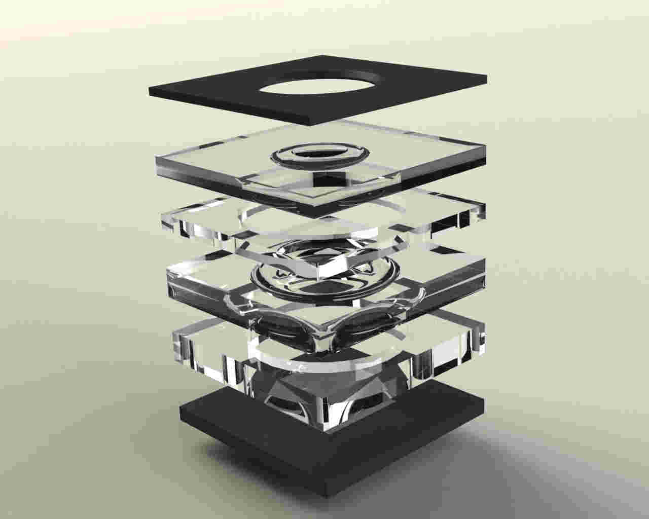
Wafer Level Optics
Wafer Level Optics
1280×837
Passion At Epic Meeting On Wafer Level Optics Passion
Passion At Epic Meeting On Wafer Level Optics Passion
1024×576

Evg Announces Nanoimprint And Wafer Level Optics System News
Evg Announces Nanoimprint And Wafer Level Optics System News
1200×932
12wafer Level Optics Schemepng Mid Atlantic Consulting Blog
12wafer Level Optics Schemepng Mid Atlantic Consulting Blog
1024×669

Wafer Level Micro Optics With Mechanical Features Meptec
Wafer Level Micro Optics With Mechanical Features Meptec
520×400

Ev Group Receives Multiple Lithography And Metrology System Orders For
Ev Group Receives Multiple Lithography And Metrology System Orders For
2953×1484

Wafer Level Optics Himax Technologies Inc
Wafer Level Optics Himax Technologies Inc
931×359

Image Sensors World Anteryon Wafer Level Optics Status
Image Sensors World Anteryon Wafer Level Optics Status
640×450


Evgroup Delo Wafer Level Optics Revolution In The Works Dvn
Evgroup Delo Wafer Level Optics Revolution In The Works Dvn
800×250

Manufacturing Wafer Level Optics Using Uv Adhesives And Polymers Tech
Manufacturing Wafer Level Optics Using Uv Adhesives And Polymers Tech
968×889

Wafer Level Optics Himax Technologies Inc
Wafer Level Optics Himax Technologies Inc
1680×500

Wafer Level Optics Introduction And Solutions Available For Wafer
Wafer Level Optics Introduction And Solutions Available For Wafer
1280×850

Wafer Level Manufacturing Wafer Level Optics Holographix Llc
Wafer Level Manufacturing Wafer Level Optics Holographix Llc
1920×305

Wafer Level Optics
Wafer Level Optics
664×498

Image Sensors World Anteryon Wafer Level Optics Status
Image Sensors World Anteryon Wafer Level Optics Status
1020×536
Wafer Level Optics
Wafer Level Optics
942×706

Precision Glass Solutions Augmented Reality Ar Glass Wafer Hpfs
Precision Glass Solutions Augmented Reality Ar Glass Wafer Hpfs
704×366

Wafer Level Optics Transmittedreflected Light Testing
Wafer Level Optics Transmittedreflected Light Testing
1260×540

Introduction And Solutions Available For Wafer Level Optics
Introduction And Solutions Available For Wafer Level Optics
950×632

Ev Group And Teramount Announce Collaboration To Implement Innovative
Ev Group And Teramount Announce Collaboration To Implement Innovative
6282×2103

Wafer Level Optics Corning
Wafer Level Optics Corning
720×720

Image Sensors World St Licenses Metalenz Wafer Level Optics
Image Sensors World St Licenses Metalenz Wafer Level Optics
1304×402
Image Sensors World St Licenses Metalenz Wafer Level Optics
Image Sensors World St Licenses Metalenz Wafer Level Optics
2048×1078

Evg Launches Automated Smartnil Nanoimprint And Wafer Level Optics System
Evg Launches Automated Smartnil Nanoimprint And Wafer Level Optics System
1200×801
Wafer Level Optics Himax Technologies Inc
Wafer Level Optics Himax Technologies Inc
1920×492

Image Sensors World Fraunhofer Institute Proposes Ultra Thin Multi
Image Sensors World Fraunhofer Institute Proposes Ultra Thin Multi
831×446

Wafer Level Optics Corning
Wafer Level Optics Corning
768×170
